A human brain is made of 100 billion cells known as neurons that help us think and remember. Similarly, computers contain billions of “brain cells” as well. They are known as transistors and they are made from silicon. Transistors have revolutionized electronics since the time they were invented by Walter Brattain, John Bardeen and William Shockley.
Semiconductors are mainly used to manufacture two devices – diodes and transistors. In all fields of electronics, transistors are used for almost all practical purposes. A transistor is an electronic device that is used for the amplification of signals, or to switch electronic signals. In this article, let us discuss junction transistors and its different types in detail.
What are Junction Transistors?
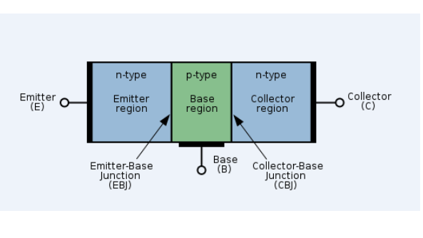
Junction transistors, also known as Bipolar Junction Transistors (BJT) consist of three terminals which are named emitter (E), Base (B)and strong>Collector (C). The transistors three-layer structure can either contain:
- an n-type semiconductor layer sandwiched between p-type layers forming a pnp configuration
or,
- a p-type layer between n-type layers forming an npn configuration.
It has two junctions between p-type and n-type semiconductors. BJTs are current-controlled devices which means that a small amount of current flowing through the base of a Bipolar Junction Transistor, results in a large current that flows from emitter to collector. In the next few sections, let us look at the actions taking place in an n-p-n transistor and a p-n-p transistor.
The action of n-p-n transistor

The n-p-n transistor consists of two n-type semiconductors that sandwich a p-type semiconductor. Here, electrons are the majority charge carriers while holes are the minority charge carriers.
In an n-p-n transistor, the majority of the charge carriers are electrons and holes are the minority charge carriers. A small amount of current at the base terminal causes a large amount of current to flow from emitter to collector. The figure below represents the circuit diagram of the n-p-n transistor:

From the circuit diagram of the n-p-n transistor, it is seen that the emitter-base circuit is forward biased while the collector-emitter circuit is reverse biased.
Due to the forward bias, the majority charge carriers in the emitter are repelled towards the base. The electron-hole recombination is very small in the base region because the base is lightly doped. Most of the electrons cross into the collector region.
The action of p-n-p transistor:

The p-n-p transistor consists of two p-type semiconductors that sandwich an n-type semiconductor. Here, holes are the majority charge carriers while electrons are the minority charge carriers.
The figure below represents the circuit diagram of the p-n-p transistor:

The emitter-base (VBE ) battery connects the p-type emitter which is forward biased whereas the collector-base (VBC ) battery connects the p-type collector which is reverse biased. In this case, the majority charge carriers in emitter are holes which are repelled towards the base. As the base layer is thin, thus only little interaction occurs when electrons and holes combine. Most of the holes reach the collector. The current is carried by holes in p-n-p transistors.
0 comments :
Post a Comment